Development of Bulk Two-Dimensional Dielectric Layer Made of Molybdenum Oxide
Since the successful separation of graphene from bulk graphite, the superior performance of graphene has attracted many scientists into the new research field of two-dimensional materials. However, although graphene has excellent carrier mobility, the use of graphene directly in field-effect transistors is severely hindered due to the gap-free structure of graphene. Alternatively, semiconductor transition metal dihalides (TMDCs) have focused on the past decade. However, for UV-related optoelectronic devices, power electronics, and dielectric layers require wide-bandgap two-dimensional materials with greater than 3 eV.
Transition metal oxide (TMO) is one of the most promising candidate materials with large band gaps, structural diversity and adjustable physical/chemical properties. However, until now, the scalable growth of atomic thin TMOs has been challenging because it is highly prone to lattice mismatch strain and strong matrix clamping during growth.
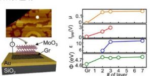
Recently, a research team led by Professor Gwan-Hyung Lee of Seoul National University has overcome this problem by adopting the van der Waals (vdW) epitaxial growth method. The research team reported nanoparticles on a graphene substrate with orthogonal molybdenum oxide (a new method for the reproducible growth of alpha-MoO). An important issue in this work is the effect of thickness on electrical and physical properties. To solve this problem, comprehensive atomic force microscopy (AFM) study was conducted to explore the structural and electrical properties of MoO3 layers of various thicknesses.
Interestingly, AFM studies have shown that even with MoO3 nanosheets having a thickness greater than 2-3 layers (1.4-2.1 nm thick), MoO3 nanosheets retain the bulk structure and electrical properties.
In particular, the thickness sensitivity of the friction is very small compared to other hexagonal two-dimensional materials. This interesting result is attributed to the fact that the double octahedral plane of the single-layer MoO3 has a very small interatomic spacing. In addition, the work function and dielectric constant are also independent of thickness, and the electron thickness structure is constant regardless of thickness.
The team also showed that MoO3 nanosheets have large current gaps and high dielectric constants, emphasizing that MoO3 can be used as a promising two-dimensional dielectric material.
For more information, please visit https://www.samaterials.com/6-molybdenum.
Cautions When Using Molybdenum Electrode Plate

Introduction to 3 Types of Molybdenum Alloys